| Number of channels (#) | 1 |
| Total supply voltage (Max) (+5V=5, +/-5V=10) | 5 |
| Total supply voltage (Min) (+5V=5, +/-5V=10) | 2.7 |
| Vos (offset voltage @ 25 C) (Max) (mV) | 0.025 |
| GBW (Typ) (MHz) | 3 |
| Features | Zero Drift |
| Slew rate (Typ) (V/us) | 4 |
| Rail-to-rail | In to V-, Out |
| Offset drift (Typ) (uV/C) | 0.015 |
| Iq per channel (Typ) (mA) | 0.919 |
| Vn at 1 kHz (Typ) (nV/rtHz) | 35 |
| CMRR (Typ) (dB) | 130 |
| Rating | Catalog |
| Operating temperature range (C) | 0 to 70 |
| Input bias current (Max) (pA) | 4 |
| Output current (Typ) (mA) | 17 |
| Architecture | CMOS |
- (For Vs = 5V, Typical Unless Otherwise Noted)
- Low Ensured Vos Over Temperature 35μV
- Low Noise with no 1/f 35nV/√Hz
- High CMRR 130dB
- High PSRR 120dB
- High AVOL 130dB
- Wide Gain-Bandwidth Product 3MHz
- High Slew Rate 4V/μs
- Low Supply Current 930μA
- Rail-to-Rail Output 30mV
- No External Capacitors Required
All trademarks are the property of their respective owners.
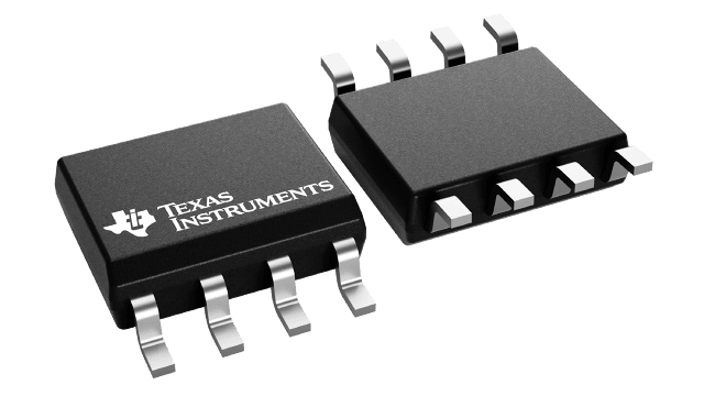
The LMV2011 is a new precision amplifier that offers unprecedented accuracy and stability at an affordable price and is offered in a miniature (5-pin SOT-23) package and in an 8-lead SOIC package. This device utilizes patented techniques to measure and continually correct the input offset error voltage. The result is an amplifier which is ultra stable over time and temperature. It has excellent CMRR and PSRR ratings, and does not exhibit the familiar 1/f voltage and current noise increase that plagues traditional amplifiers. The combination of the LMV2011 characteristics makes it a good choice for transducer amplifiers, high gain configurations, ADC buffer amplifiers, DAC I-V conversion, and any other 2.7V-5V application requiring precision and long term stability.
Other useful benefits of the LMV2011 are rail-to-rail output, a low supply current of 930μA, and wide gain-bandwidth product of 3MHz. These extremely versatile features found in the LMV2011 provide high performance and ease of use.


