| Sample rate (Max) (MSPS) | 65 |
| Resolution (Bits) | 12 |
| Number of input channels | 2 |
| Interface type | Parallel CMOS |
| Analog input BW (MHz) | 300 |
| Features | Low Power |
| Rating | Catalog |
| Input range (Vp-p) | 2 |
| Power consumption (Typ) (mW) | 335 |
| Architecture | Pipeline |
| SNR (dB) | 70.7 |
| ENOB (Bits) | 11.3 |
| SFDR (dB) | 86 |
| Operating temperature range (C) | -40 to 85 |
| Input buffer | No |
- Single +3.3V Supply
- High SNR: 70.7dBFS at fIN = 5MHz
- Total Power Dissipation:
Internal Reference: 371mW
External Reference: 335mW - Internal or External Reference
- Low DNL: ±0.3LSB
- Flexible Input Range: 1.5VPP to 2VPP
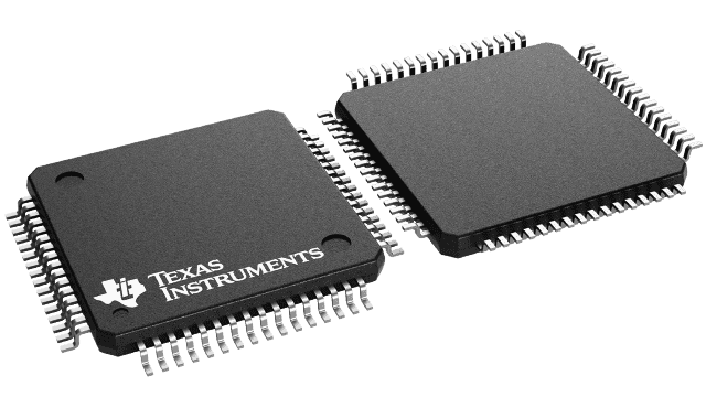
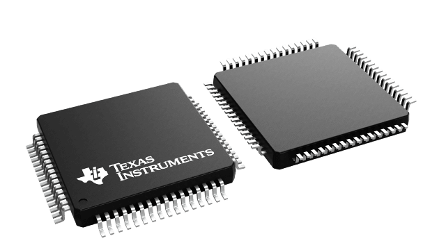
- TQFP-64 Package
- APPLICATIONS
- Communications IF Processing
- Communications Base Stations
- Test Equipment
- Medical Imaging
- Video Digitizing
- CCD Digitizing
All trademarks are the property of their respective owners.
The ADS5232 is a dual, high-speed, high dynamic range, 12-bit pipelined analog-to-digital converter (ADC). This converter includes a high-bandwidth sample-and-hold amplifier that gives excellent spurious performance up to and beyond the Nyquist rate. The differential nature of the sample-and-hold amplifier and ADC circuitry minimizes even-order harmonics and gives excellent common-mode noise immunity.
The ADS5232 provides for setting the full-scale range of the converter without any external reference circuitry. The internal reference can be disabled, allowing low-drive, external references to be used for improved tracking in multichannel systems.
The ADS5232 provides an over-range indicator flag to indicate an input signal that exceeds the full-scale input range of the converter. This flag can be used to reduce the gain of front-end gain control circuitry. There is also an output enable pin to allow for multiplexing and testing on a PC board.
The ADS5232 employs digital error correction techniques to provide excellent differential linearity for demanding imaging applications. The ADS5232 is available in a TQFP-64 package.


