| Resolution (Bits) | 16 |
| Number of input channels | 1 |
| Sample rate (Max) (kSPS) | 1250 |
| Interface type | Serial |
| Architecture | Delta-Sigma |
| Input type | Differential |
| Rating | Catalog |
| Reference mode | Ext, Int |
| Input range (Max) (V) | 4.6 |
| Input range (Min) (V) | 0 |
| Operating temperature range (C) | -40 to 85 |
| Power consumption (Typ) (mW) | 330 |
| Analog voltage AVDD (Min) (V) | 4.75 |
| SNR (dB) | 91 |
| Analog voltage AVDD (Max) (V) | 5.25 |
| INL (Max) (+/-LSB) | 0.75 |
| Digital supply (Min) (V) | 2.7 |
| Digital supply (Max) (V) | 5.25 |
- High Speed:
- Data Rate: 1.25MSPS
- Bandwidth: 615kHz
- Outstanding Performance:
- SNR: 92dB at fIN = 100kHz, –1dBFS
- THD: –103dB at fIN = 100kHz, –6dBFS
- SFDR: 105dB at fIN = 100kHz, –6dBFS
- Ease-of-Use:
- High-Speed 3-Wire Serial Interface
- Directly Connects to TMS320 DSPs
- On-Chip Digital Filter Simplifies Anti-Alias Requirements
- Simple Pin-Driven Control—No On-Chip Registers to Program
- Selectable On-Chip Voltage Reference
- Simultaneous Sampling with Multiple ADS1601s
- Low Power:
- 330mW at 1.25MSPS
- 145mW at 625kSPS
- Power-Down Mode
The ADS1601 is a high-speed, high-precision, delta-sigma analog-to-digital converter (ADC) manufactured on an advanced CMOS process. The ADS1601 oversampling topology reduces clock jitter sensitivity during the sampling of high-frequency, large amplitude signals by a factor of four over that achieved by Nyquist-rate ADCs. Consequently, signal-to-noise ratio (SNR) is particularly improved. Total harmonic distortion (THD) is –103dB, and the spurious-free dynamic range (SFDR) is 105dB
Optimized for power and performance, the ADS1601 dissipates only 330mW while providing a full-scale differential input range of ±0.94VREF. Having such a wide input range makes out-of-range signals uncommon. The OTR pin indicates if an analog input out-of-range condition does occur. The differential input signal is measured against the differential reference, which can be generated internally on the ADS1601 or supplied externally.
The ADS1601 uses an inherently stable advanced modulator with an on-chip decimation filter. The filter stop band extends to 19.3MHz, which greatly simplifies the anti-aliasing circuitry. The modulator samples the input signal up to 20MSPS, depending on fCLK, while the 16x decimation filter uses a series of four half-band FIR filter stages to provide 75dB of stop band attenuation and 0.001dB of passband ripple.
Output data is provided over a simple 3-wire serial interface at rates up to 1.25MSPS, with a –3dB bandwidth of 615kHz. The output data or its complementary format directly connects to DSPs such as TI’s TMS320 family, FPGAs, or ASICs. A dedicated synchronization pin enables simultaneous sampling with multiple ADS1601s in multi-channel systems. Power dissipation is set by an external resistor that allows a reduction in dissipation when operating at slower speeds. All of the ADS1601 features are controlled by dedicated I/O pins, which simplify operation by eliminating the need for on-chip registers.
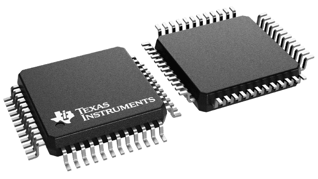
The high performing, easy-to-use ADS1601 is especially suitable for demanding measurement applications in sonar, vibration analysis, and data acquisition. The ADS1601 is offered in a small, 7mm × 7mm TQFP-48 package and is specified from –40°C to +85°C.


