

| Resolution (Bits) | 14 |
| Number of DAC channels (#) | 1 |
| Interface type | Parallel CMOS |
| Sample/update rate (MSPS) | 125 |
| Features | Low Power |
| Rating | Catalog |
| Interpolation | 1x |
| Power consumption (Typ) (mW) | 175 |
| SFDR (dB) | 82 |
| Architecture | Current Source |
| Operating temperature range (C) | -40 to 85 |
| Reference type | Ext |
- Member of the Pin-Compatible CommsDAC? Product Family
- 125 MSPS Update Rate
- 14-Bit Resolution
- Spurious Free Dynamic Range (SFDR) to Nyquist at 40 MHz Output: 63 dBc
- 1 ns Setup/Hold Time
- Differential Scalable Current Outputs: 2 mA to 20 mA
- On-Chip 1.2 V Reference
- 3 V and 5 V CMOS-Compatible Digital Interface
- Straight Binary or Twos Complement Input
- Power Dissipation: 175 mW at 5 V, Sleep Mode: 25 mW at 5 V
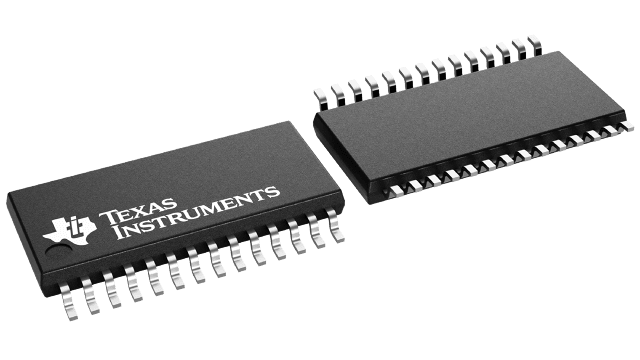
- Package: 28-Pin SOIC and TSSOP
CommsDAC is a trademark of Texas Instruments Incorporated.
The THS5671A is a 14-bit resolution digital-to-analog converter (DAC) specifically optimized for digital data transmission in wired and wireless communication systems. The 14-bit DAC is a member of the CommsDAC series of high-speed, low-power CMOS digital-to-analog converters. The CommsDAC family consists of pin compatible 14-, 12-, 10-, and 8-bit DACs. All devices offer identical interface options, small outline package, and pinout. The THS5671A offers superior ac and dc performance while supporting update rates up to 125 MSPS.
The THS5671A operates from an analog supply of 4.5 V to 5.5 V. Its inherent low power dissipation of 175 mW ensures that the device is well-suited for portable and low-power applications. Lowering the full-scale current output reduces the power dissipation without significantly degrading performance. The device features a SLEEP mode, which reduces the standby power to approximately 25 mW, thereby optimizing the power consumption for system needs.
The THS5671A is manufactured in Texas Instruments advanced high-speed mixed-signal CMOS process. A current-source-array architecture combined with simultaneous switching shows excellent dynamic performance. On-chip edge-triggered input latches and a 1.2 V temperature-compensated bandgap reference provide a complete monolithic DAC solution. The digital supply range of 3 V to 5.5 V supports 3 V and 5 V CMOS logic families. Minimum data input setup and hold times allow for easy interfacing with external logic. The THS5671A supports both a straight binary and twos complement input word format, enabling flexible interfacing with digital signal processors.
The THS5671A provides a nominal full-scale differential output current of 20 mA and < 300 kΩ output impedance, supporting both single-ended and differential applications. The output current can be directly fed to the load (e.g., external resistor load or transformer), with no additional external output buffer required. An accurate on-chip reference and control amplifier allows the user to adjust this output current from 20 mA down to 2 mA, with no significant degradation of performance. This reduces power consumption and provides 20 dB gain range control capabilities. Alternatively, an external reference voltage and control amplifier may be applied in applications using a multiplying DAC. The output voltage compliance range is 1.25 V.
The THS5671A is available in both a 28-pin SOIC and TSSOP package. The device is characterized for operation over the industrial temperature range of ?40°C to 85°C.


