


| DSP | 1 C55x |
| DSP MHz (Max) | 108 |
| CPU | 16-bit |
| Operating system | DSP/BIOS, VLX |
| Rating | Catalog |
| Operating temperature range (C) | -40 to 85 |
- High-Performance, Low-Power, Fixed-Point TMS320C55x? Digital Signal Processor
- 9.26-ns Instruction Cycle Time
- 108-MHz Clock Rate
- One/Two Instruction(s) Executed per Cycle
- Dual Multipliers [Up to 216 Million Multiply-Accumulates per Second (MMACS)]
- Two Arithmetic/Logic Units (ALUs)
- Three Internal Data/Operand Read Buses and Two Internal Data/Operand Write Buses
- 64K x 16-Bit On-Chip RAM, Composed of:
- 64K Bytes of Dual-Access RAM (DARAM) 8 Blocks of 4K × 16-Bit
- 64K Bytes of Single-Access RAM (SARAM) 8 Blocks of 4K × 16-Bit
- On-Chip Bootloader
- 8M × 16-Bit Maximum Addressable External Memory Space (Synchronous DRAM)
- 16-Bit External Memory Interface (EMIF) With GPIO Capabilities and Glueless Interface to:
- Asynchronous Static RAM (SRAM)
- Asynchronous EPROM
- Synchronous DRAM (SDRAM)
- Programmable Low-Power Control of Six Device Functional Domains
- On-Chip Scan-Based Emulation Logic
- On-Chip Peripherals
- Two 20-Bit Timers
- Watchdog Timer
- Six-Channel Direct Memory Access (DMA) Controller
- Three Multichannel Buffered Serial Ports (McBSPs)
- Programmable Phase-Locked Loop Clock Generator
- Seven (LQFP) or Eight (BGA) General-Purpose I/O (GPIO) Pins and a General-Purpose Output Pin (XF)
- USB Full-Speed (12 Mbps) Slave Port Supporting Bulk, Interrupt and Isochronous Transfers
- Inter-Integrated Circuit (I2C) Multi-Master and Slave Interface
- Real-Time Clock (RTC) With Crystal Input, Separate Clock Domain, Separate Power Supply
- IEEE Std 1149.1
 (JTAG) Boundary Scan Logic
 - Packages:
- 144-Terminal Low-Profile Quad Flatpack (LQFP) (PGE Suffix)
- 179-Terminal MicroStar BGA? (Ball Grid Array) (GHH and ZHH Suffixes)
- 1.2-V Core (108 MHz), 2.7-V - 3.6-V I/Os
All trademarks are the property of their respective owners.
TMS320C55x and MicroStar BGA are trademarks of Texas Instruments. IEEE Standard 1149.1-1990 Standard-Test-Access Port and Boundary Scan Architecture.
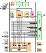
The TMS320VC5506 fixed-point digital signal processor (DSP) is based on the TMS320C55x DSP generation CPU processor core. The C55x? DSP architecture achieves high performance and low power through increased parallelism and total focus on reduction in power dissipation. The CPU supports an internal bus structure that is composed of one program bus, three data read buses, two data write buses, and additional buses dedicated to peripheral and DMA activity. These buses provide the ability to perform up to three data reads and two data writes in a single cycle. In parallel, the DMA controller can perform up to two data transfers per cycle independent of the CPU activity.
The C55x CPU provides two multiply-accumulate (MAC) units, each capable of 17-bit x 17-bit multiplication in a single cycle. A central 40-bit arithmetic/logic unit (ALU) is supported by an additional 16-bit ALU. Use of the ALUs is under instruction set control, providing the ability to optimize parallel activity and power consumption. These resources are managed in the Address Unit (AU) and Data Unit (DU) of the C55x CPU.
The C55x DSP generation supports a variable byte width instruction set for improved code density. The Instruction Unit (IU) performs 32-bit program fetches from internal or external memory and queues instructions for the Program Unit (PU). The Program Unit decodes the instructions, directs tasks to AU and DU resources, and manages the fully protected pipeline. Predictive branching capability avoids pipeline flushes on execution of conditional instructions.
The 128K bytes of on-chip memory on 5506 is sufficient for many hand-held appliances, portable GPS systems, wireless speaker phones, portable PDAs, and gaming devices. Many of these appliances typically require 64K bytes or more on-chip memory but less than 128K bytes of memory, and need to operate in standby mode for more than 60% to 70% of time. For the applications which require more than 128K bytes of on-chip memory but less than 256K bytes of on-chip memory, Texas Instruments (TI) offers the TMS320VC5509A device, which is based on the TMS320C55x DSP core.
The 5506 peripheral set includes an external memory interface (EMIF) that provides glueless access to asynchronous memories like EPROM and SRAM, as well as to high-speed, high-density memories such as synchronous DRAM. Additional peripherals include Universal Serial Bus (USB), real-time clock, watchdog timer, and I2C multi-master and slave interface. Three full-duplex multichannel buffered serial ports (McBSPs) provide glueless interface to a variety of industry-standard serial devices, and multichannel communication with up to 128 separately enabled channels. The DMA controller provides data movement for six independent channel contexts without CPU intervention, providing DMA throughput of up to two 16-bit words per cycle. Two general-purpose timers, up to eight dedicated general-purpose I/O (GPIO) pins, and digital phase-locked loop (DPLL) clock generation are also included.
The 5506 is supported by the industry?s award-winning eXpressDSP?, Code Composer Studio? Integrated Development Environment (IDE), DSP/BIOS?, Texas Instruments? algorithm standard, and the industry?s largest third-party network. The Code Composer Studio IDE features code generation tools including a C Compiler and Visual Linker, simulator, RTDX?, XDS510?, XDS560?, emulation device drivers, and evaluation modules. The 5506 is also supported by the C55x DSP Library which features more than 50 foundational software kernels (FIR filters, IIR filters, FFTs, and various math functions) as well as chip and board support libraries.


