

| DSP | 1 C67x |
| DSP MHz (Max) | 167, 200, 200, 225, 300 |
| CPU | 32-/64-bit |
| Operating system | DSP/BIOS |
| Rating | Catalog |
| Operating temperature range (C) | -40 to 105, 0 to 90 |
- Highest-Performance Floating-Point Digital Signal Processor (DSP): TMS320C6713B
- Eight 32-Bit Instructions/Cycle
- 32/64-Bit Data Word
- 300-, 225-, 200-MHz (GDP and ZDP), and 225-, 200-, 167-MHz (PYP) Clock Rates
- 3.3-, 4.4-, 5-, 6-Instruction Cycle Times
- 2400/1800, 1800/1350, 1600/1200, and 1336/1000 MIPS/MFLOPS
- Rich Peripheral Set, Optimized for Audio
- Highly Optimized C/C++ Compiler
- Extended Temperature Devices Available
- Advanced Very Long Instruction Word (VLIW) TMS320C67x? DSP Core
- Eight Independent Functional Units:
- 2 ALUs (Fixed-Point)
- 4 ALUs (Floating-/Fixed-Point)
- 2 Multipliers (Floating-/Fixed-Point)
- Load-Store Architecture With 32 32-Bit General-Purpose Registers
- Instruction Packing Reduces Code Size
- All Instructions Conditional
- Eight Independent Functional Units:
- Instruction Set Features
- Native Instructions for IEEE 754
- Single- and Double-Precision
- Byte-Addressable (8-, 16-, 32-Bit Data)
- 8-Bit Overflow Protection
- Saturation; Bit-Field Extract, Set, Clear; Bit-Counting; Normalization
- Native Instructions for IEEE 754
- L1/L2 Memory Architecture
- 4K-Byte L1P Program Cache (Direct-Mapped)
- 4K-Byte L1D Data Cache (2-Way)
- 256K-Byte L2 Memory Total: 64K-Byte L2 Unified Cache/Mapped RAM, and 192K-Byte Additional L2 Mapped RAM
- Device Configuration
- Boot Mode: HPI, 8-, 16-, 32-Bit ROM Boot
- Endianness: Little Endian, Big Endian
- 32-Bit External Memory Interface (EMIF)
- Glueless Interface to SRAM, EPROM, Flash, SBSRAM, and SDRAM
- 512M-Byte Total Addressable External Memory Space
- Enhanced Direct-Memory-Access (EDMA) Controller (16 Independent Channels)
- 16-Bit Host-Port Interface (HPI)
- Two McASPs
- Two Independent Clock Zones Each (1 TX and 1 RX)
- Eight Serial Data Pins Per Port: Individually Assignable to any of the Clock Zones
- Each Clock Zone Includes:
- Programmable Clock Generator
- Programmable Frame Sync Generator
- TDM Streams From 2-32 Time Slots
- Support for Slot Size:
- 8, 12, 16, 20, 24, 28, 32 Bits
- Data Formatter for Bit Manipulation
- Wide Variety of I2S and Similar Bit Stream Formats
- Integrated Digital Audio Interface Transmitter (DIT) Supports:
- S/PDIF, IEC60958-1, AES-3, CP-430 Formats
- Up to 16 transmit pins
- Enhanced Channel Status/User Data
- Extensive Error Checking and Recovery
- Two Inter-Integrated Circuit Bus (I2C Bus?) Multi-Master and Slave Interfaces
- Two Multichannel Buffered Serial Ports:
- Serial-Peripheral-Interface (SPI)
- High-Speed TDM Interface
- AC97 Interface
- Two 32-Bit General-Purpose Timers
- Dedicated GPIO Module With 16 pins (External Interrupt Capable)
- Flexible Phase-Locked-Loop (PLL) Based Clock Generator Module
- IEEE-1149.1 (JTAG
 ) Boundary-Scan-Compatible
 - 208-Pin PowerPAD? PQFP (PYP)
- 272-BGA Packages (GDP and ZDP)
- 0.13-μm/6-Level Copper Metal Process
- CMOS Technology
- 3.3-V I/Os, 1.2
 -V Internal (GDP/ZDP/ PYP)
 - 3.3-V I/Os, 1.4-V Internal (GDP/ZDP) [300 MHz]
TMS320C67x and PowerPAD are trademarks of Texas Instruments.
I2C Bus is a trademark of Philips Electronics N.V. Corporation
All trademarks are the property of their respective owners. IEEE Standard 1149.1-1990 Standard-Test-Access Port and Boundary Scan Architecture. These values are compatible with existing 1.26-V designs.
TMS320C6000, eXpressDSP, Code Composer Studio, and DSP/BIOS are trademarks of Texas Instruments. Throughout the remainder of this document, TMS320C6713B shall be referred to as C6713B or 13B.
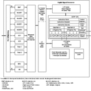
The TMS320C67x? DSPs (including the TMS320C6713B device) compose the floating-point DSP generation in the TMS320C6000? DSP platform. The C6713B device is based on the high-performance, advanced very-long-instruction-word (VLIW) architecture developed by Texas Instruments (TI), making this DSP an excellent choice for multichannel and multifunction applications.
Operating at 225 MHz, the C6713B delivers up to 1350 million floating-point operations per second (MFLOPS), 1800 million instructions per second (MIPS), and with dual fixed-/floating-point multipliers up to 450 million multiply-accumulate operations per second (MMACS).
Operating at 300 MHz, the C6713B delivers up to 1800 million floating-point operations per second (MFLOPS), 2400 million instructions per second (MIPS), and with dual fixed-/floating-point multipliers up to 600 million multiply-accumulate operations per second (MMACS).
The C6713B uses a two-level cache-based architecture and has a powerful and diverse set of peripherals. The Level 1 program cache (L1P) is a 4K-byte direct-mapped cache and the Level 1 data cache (L1D) is a 4K-byte 2-way set-associative cache. The Level 2 memory/cache (L2) consists of a 256K-byte memory space that is shared between program and data space. 64K bytes of the 256K bytes in L2 memory can be configured as mapped memory, cache, or combinations of the two. The remaining 192K bytes in L2 serves as mapped SRAM.
The C6713B has a rich peripheral set that includes two Multichannel Audio Serial Ports (McASPs), two Multichannel Buffered Serial Ports (McBSPs), two Inter-Integrated Circuit (I2C) buses, one dedicated General-Purpose Input/Output (GPIO) module, two general-purpose timers, a host-port interface (HPI), and a glueless external memory interface (EMIF) capable of interfacing to SDRAM, SBSRAM, and asynchronous peripherals.
The two McASP interface modules each support one transmit and one receive clock zone. Each of the McASP has eight serial data pins which can be individually allocated to any of the two zones. The serial port supports time-division multiplexing on each pin from 2 to 32 time slots. The C6713B has sufficient bandwidth to support all 16 serial data pins transmitting a 192 kHz stereo signal. Serial data in each zone may be transmitted and received on multiple serial data pins simultaneously and formatted in a multitude of variations on the Philips Inter-IC Sound (I2S) format.
In addition, the McASP transmitter may be programmed to output multiple S/PDIF, IEC60958, AES-3, CP-430 encoded data channels simultaneously, with a single RAM containing the full implementation of user data and channel status fields.
The McASP also provides extensive error-checking and recovery features, such as the bad clock detection circuit for each high-frequency master clock which verifies that the master clock is within a programmed frequency range.
The two I2C ports on the TMS320C6713B allow the DSP to easily control peripheral devices and communicate with a host processor. In addition, the standard multichannel buffered serial port (McBSP) may be used to communicate with serial peripheral interface (SPI) mode peripheral devices.
The TMS320C6713B device has two bootmodes: from the HPI or from external asynchronous ROM. For more detailed information, see the bootmode section of this data sheet.
The TMS320C67x DSP generation is supported by the TI eXpressDSP? set of industry benchmark development tools, including a highly optimizing C/C++ Compiler, the Code Composer Studio? Integrated Development Environment (IDE), JTAG-based emulation and real-time debugging, and the DSP/BIOS? kernel.


