
| Vin (Min) (V) | 1.8 |
| Vin (Max) (V) | 5.5 |
| Vout (Min) (V) | 5 |
| Vout (Max) (V) | 5 |
| Switch current limit (Typ) (A) | 4 |
| Regulated outputs (#) | 1 |
| Switching frequency (Min) (kHz) | 500 |
| Switching frequency (Max) (kHz) | 700 |
| Iq (Typ) (mA) | 0.02 |
| Features | Synchronous Rectification |
| Duty cycle (Max) (%) | 100 |
| Rating | Catalog |
- 96% Efficient Synchronous Boost Converter With
1000-mA Output Current From 1.8-V Input - Device Quiescent Current: 20-μA (Typ)
- Input Voltage Range: 1.8-V to 5.5-V
- Fixed and Adjustable Output Voltage Options Up
to 5.5-V - Power Save Mode for Improved Efficiency at Low
Output Power - Low Battery Comparator
- Low EMI-Converter (Integrated Antiringing Switch)
- Load Disconnect During Shutdown
- Over-Temperature Protection
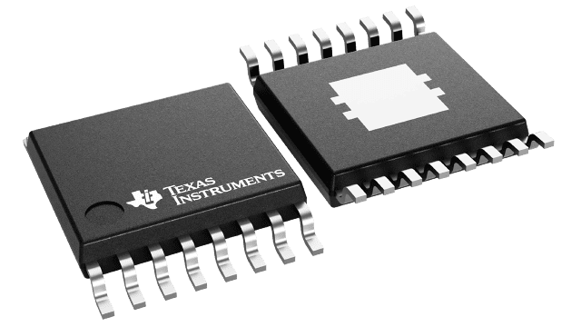
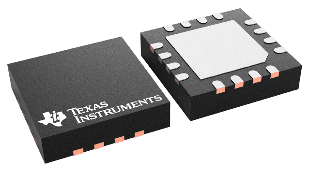
- Available in a Small 4 mm × 4 mm QFN-16 or in a
TSSOP-16 Package
The TPS6103x devices provide a power supply solution for products powered by either a one-cell Li-Ion or Li-polymer, or a two to three-cell alkaline, NiCd or NiMH battery. The converter generates a stable output voltage that is either adjusted by an external resistor divider or fixed internally on the chip. It provides high efficient power conversion and is capable of delivering output currents up to 1 A at 5 V at a supply voltage down to 1.8 V. The implemented boost converter is based on a fixed frequency, pulse-width- modulation (PWM) controller using a synchronous rectifier to obtain maximum efficiency. At low load currents the converter enters Power Save mode to maintain a high efficiency over a wide load current range. The Power Save mode can be disabled, forcing the converter to operate at a fixed switching frequency. It can also operate synchronized to an external clock signal that is applied to the SYNC pin. The maximum peak current in the boost switch is limited to a value of 4500 mA.
The converter can be disabled to minimize battery drain. During shutdown, the load is completely disconnected from the battery. A low-EMI mode is implemented to reduce ringing and, in effect, lower radiated electromagnetic energy when the converter enters the discontinuous conduction mode.


